
Symbolic view allows you to create and see the symbol for a logic device. So once you have created your standard cells and want to combine them into larger circuit, you can see them by their logic symbol and not just on the transistor level.
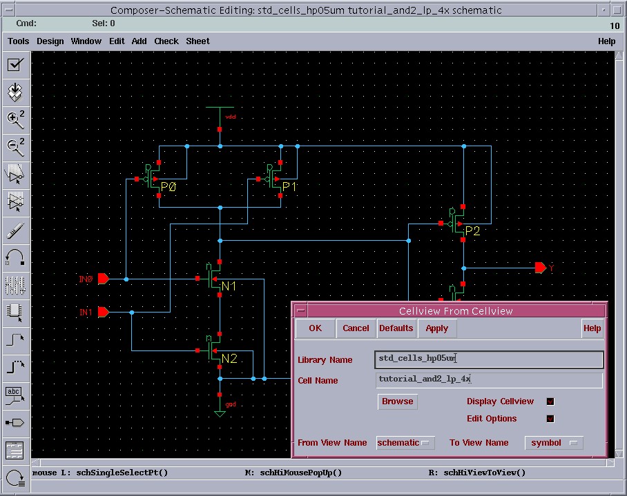
1. Once you have completed you standard cell on the transistor level, we will want to create a symbol for it. Form the schematic view go Design >> Create Cellview >> From Cellview

2. Hit Ok and a new window will pop up. Make sure everything is correct. Name the input and output pins.

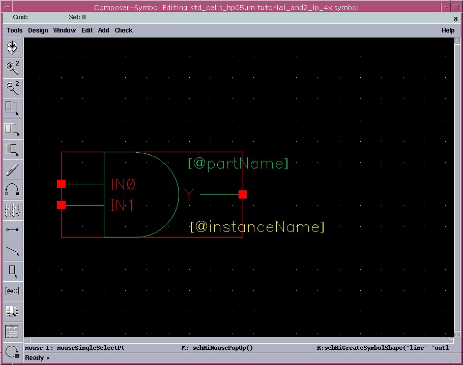
3. We now will come to the symbol editing window. Here we will draw the symbol, in our case a AND gate. Delete the green box by selecting it and hitting the Del key. Just a note that once you press the Del key you are in delete mode and must press Esc to get out.

4. Now we can begin to draw the AND gate. Using the draw button we can draw different shapes, play around with the different shapes to become familiar with each tool. Use this button to draw the shapes.
![]()

5. Draw the symbol for an AND gate, however you like. Making sure the the red boxes of the pins touch the red line incompassing the symbol, as shown in the pictures.

Save the symbol with this button.
![]()
Cadence is a trademark of Cadence Design Systems, Inc., 555 River Oaks Parkway, San Jose, CA 95134
Synopsys is a trademark of Synopsys Inc, 700 East Middlefield Rd. Mountain View, CA 94043